
Semiconductor Capital Equipment Overview : Part III (Back End Assembly)
Semiconductor Capital Equipment Overview : Part III (Back End Assembly)
Semiconductor Back End Assembly/Packaging Capital Equipment Suppliers

Back End Assembly Capital Equipment Suppliers
The semiconductor manufacturing process involves two distinct phases: wafer processing, commonly referred to as the front-end, and assembly and test operations, commonly referred to as the back-end. Front end and process control equipment were covered in the last 2 parts:
Semiconductor Front End Capital Equipment Overview: Part I
Semiconductor Front End Capital Equipment Overview: Part II
Assemblies or packages provide the electronic interface and physical connection between a semiconductor device, or chip, and other electronic components and protect the chip from the external environment.

VLSI Research estimated that the size of the assembly equipment market was approximately $ 3.6 billion in 2020, or 5% of the total semiconductor equipment market.
Polymath Pursuit had already written an excellent article on Assembly/Packaging equipment. In this article, I will cover assembly equipment technology, process, market trends and ecosystem.

Assembly/Packaging Technologies
Semiconductor assembly equipment involves three primary process technologies depending on the product application required:
Leadframe assembly, the most traditional approach, involves the electrical connection of the chip via a wire bonding process to a metal leadframe. Leadframe assembly technology is most frequently used to produce semiconductor devices for mass market and consumer electronics applications. Leadframe assembly use wirebond or flip chip technology to interconnect a die to a leadframe package carrier. Two of the most popular traditional leadframe package types are small outline integrated circuit and quad flat package, commonly known as “dual” and “quad” products, respectively, based upon the number of sides from which the leads extend.
Wire bonding is one of the major interconnect technologies in packaging. A wire bonder stitches one chip to another chip or substrate using tiny wires. Wire bonding is used for low-cost legacy packages, midrange packages, and memory die stacking.
There are two main types of wire bonders—ball bonding and wedge bonding. Over 90% of the market uses ball bonding and wedge bonding is used for discrete products and power devices with heavy wire.
Substrate assembly has gained increased market acceptance over the past decade. It is used most frequently in new product applications that require high degrees of miniaturization and chip density such as smart phones, servers, tablets and laptops as well as wireless, automotive and cloud-based internet applications. In a typical substrate assembly, no metal leadframes are utilized and the electrical connection of the chip is made directly to a multi-layer substrate or through the creation of direct connections to the multi-layer substrate via a flip chip die bonding process. Some of the assembly/packages in this category include stacked chip scale packages (CSP), wirebond ball grid array (BGA) packages and plastic ball grid array (PBGA) packages.
Stacked CSP technology enables the stacking of a wide range of different semiconductor devices to deliver high levels of silicon integration and area efficiency. Stacked CSP is ideal for memory and mixed signal applications.
Wirebond ball grid array packages offer a broad selection of ball array pitches, ball counts and body sizes, single and multi-die layouts, stacked die and passive component integration.
PBGA packages are used in applications requiring higher pin count than leadframe packages, but typically have lower pin counts than flip chip. PBGA packages are designed for low inductance, improved thermal operation and enhanced surface-mount technology ability.
Wafer level packaging, the most advanced assembly technology, eliminates the use of either a metal leadframe or laminated substrate for semiconductor assembly. In wafer level packaging, the electrical connections are directly applied to the chip without the need for an interposer. This process technology enables customers to achieve an even higher degrees of miniaturization, chip density and performance. This lowers the energy consumption as compared to substrate assembly but at a higher cost and reduced yield. It is anticipated that wafer level packaging will be more actively utilized for next generation applications such as data mining, predictive analytical software, artificial intelligence, high performance computing and new 5G powered systems and services as we move further towards the digital society.

Advanced packaging solutions for mass reflow include flip chip, wafer level packaging (WLP), fan-out wafer level packaging (FOWLP), advanced package-on-package, embedded die, and System-in-Package (SiP). Advanced packaging applications have grown significantly over past decade and ~40% of wafers use advanced packaging interconnects. This is the leading growth segment of assembly equipment market. Flip chip and WLP are the leading advanced packaging assembly processes over the next five years.
Assembly/Packaging Process
Assembly process is broadly divided into Wire Bonding, Die Attach, Packaging, Plating, Dicing and Inspection process.
As per VLSI Research, Die Attach systems represented the largest estimated portion of the assembly equipment market in 2020 (31%) followed by Wire Bond (22%), Packaging (16%) and Plating (1%). Package/Die Inspection, Dicing and Other contributes the remaining 34%.

Wire Bonding equipment: thermosonic bonding, ultrasonic bonding, thermocompression bonding, ball bonder and wedge bonder
Die attach equipment: single chip, multi chip, multi module, flip chip, TCB, FOWLP and hybrid die bonding systems and die sorting systems.
Packaging equipment: conventional, ultra thin and wafer level molding, trim and form and singulation systems
Plating equipment: tin, copper, precious metal and solar plating systems and related process chemicals
Dicing equipment: blade dicing, plasma dicing, laser dicing, backside grinding
Assembly equipment market trend
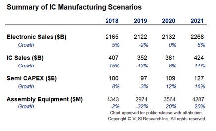
Assembly Equipment sales bounced back from 2018 and 2019 under investment, reaching over $4.2B in 2021 with two consecutive year growth of 20%.
In 2020, bonding equipment had a strong year with sales jumping 25%. Ball bonding outperformed their peers, soaring 69% followed by Die bonding up by 13%. Companies that performed well in these segments were: BE Semiconductor Industries, ASM Pacific Technology, Kulicke & Soffa, Fasford Technology, Shinkawa, and Hoson.

The below chart shows the latest Assembly Equipment sales including the $800M hybrid bonding forecast beginning 2021. The hybrid bonding market will be one of top three assembly equipment market along with Wire bonding and Die bonding.

Assembly equipment Ecosystem
Customers of assembly equipment are either independent device manufacturers (IDMs) which purchase equipment for internal use at their production facilities or subcontractors including OSATs (Outsourced Semiconductor Assembly and Test) which purchase equipment to assemble packages for third parties on a contract basis.
Assembly equipment subcontractors include both OSATs and Foundries like ASE, Amkor, Forehope, Foxconn, Greatek, Huatian, Infineon, JCET/STATS ChipPAC & LG Innotek and IDMs like Micron, NXP, STMicroelectronics & TDK Electronics and .

BE Semiconductor
Nasdaq Symbol: BESIY, Market Cap: $6.806 billion, LTM Revenue: $0.569 billion, Gross Margins: 59.8%, Operating Margins:37.0%, Net Margin: 32.1%
BE Semiconductor (Besi) offers products and services for Die Attach equipment, Packaging equipment and Plating equipment. Besi is a leading provider of advanced packaging solutions to customers which incorporate both substrate and wafer level based packaging processes in their assembly operations.

Kulicke & Soffa
Nasdaq Symbol: KLIC, Market Cap: $3.390 billion, LTM Revenue: $0.936 billion, Gross Margins: 45.7%, Operating Margins: 17.7%, Net Margin: 15.7%
Kulicke and Soffa Industries designs, manufactures, and sells capital equipment and tools to assemble semiconductor devices. The Capital Equipment segment manufactures and sells ball and wedge bonders, and advanced packaging and electronic assembly solutions.

Stock Performance and Fundamentals
Semiconductor assembly equipment market is much more cyclic than the front end equipment market. Assembly equipment went through an under investment in 2018 & 2019 and the industry is bouncing back in the last 2 years.
BE Semiconductors has strong margins and trading at a forward PE multiple of 18.6x. It’s long term prospects is on the advance packaging market.
Kulicke & Soffa is a dominant player in the wire bonding market which grew by 69% in 2020 to reach $800 million. The headwind for KLIC from a long term investment perspective is the low 6% wire bonding equipment market growth and a less than 10% advanced packaging revenue share.
Below is a comparison on stock performance of major assembly equipment suppliers along with #2 OSAT customer over last 10 years.


In the upcoming Semiconductor Capital Equipment Overview: Part IV, we will discuss the back end test equipment technology.