
Semiconductor Capital Equipment Overview : Part II
Semiconductor Capital Equipment Overview : Part II
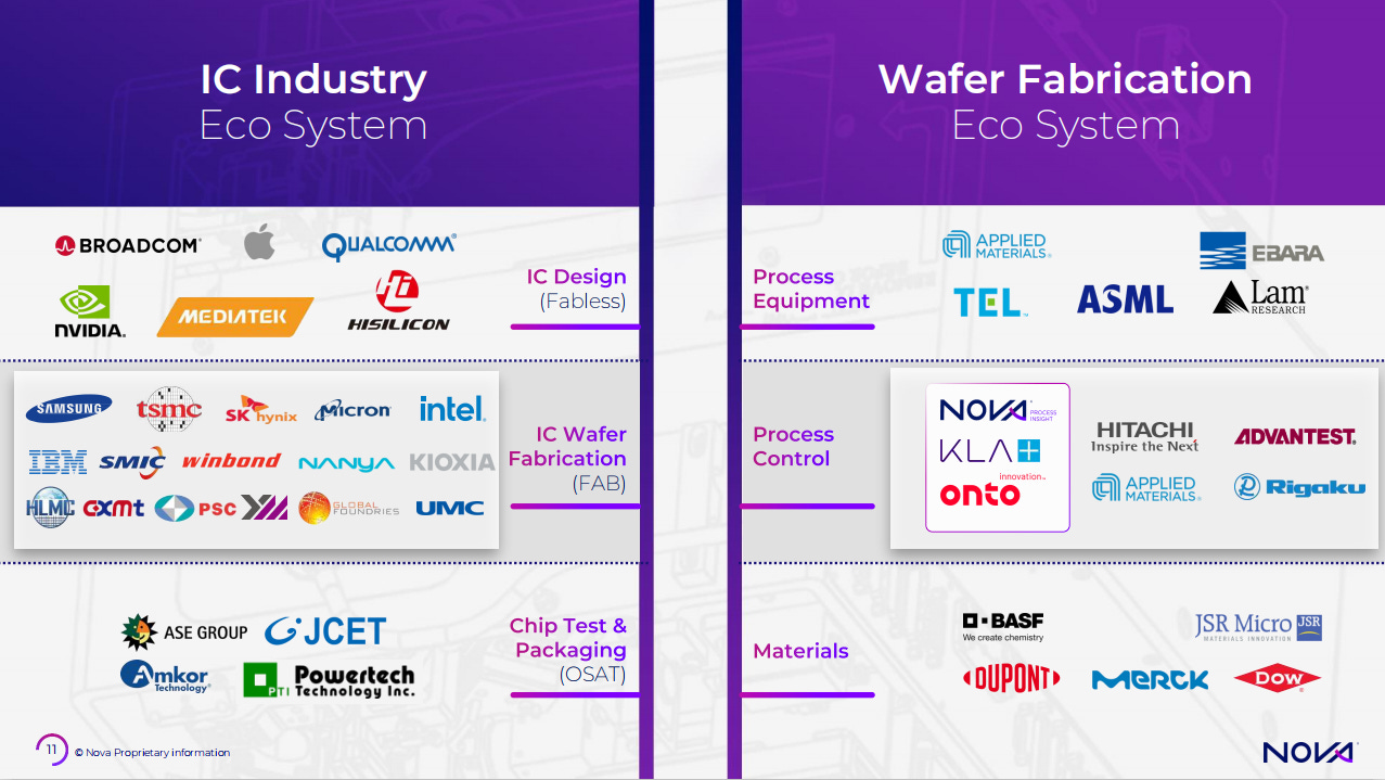
Semiconductor Process Control Equipment Overview

Process Control Equipment Market
We covered front end equipment in our last series on Semiconductor Front End Capital Equipment Overview such as Photolithography, Deposition, Etching, Cleaning, Ion Implantation, Chemical-Mechanical Planarization and Process Control Equipment. Front end covers 85% of the WFE market of $71.8 billion projection for 2021. These key process steps rely on metrology systems to monitor film thickness, uniformity, and critical dimensions and material characteristics, to ensure the correct result has been achieved. The measurements taken by metrology systems during the manufacturing process help ensure process uniformity and help semiconductor manufacturers avoid costly rework and misprocessing, therefore increasing efficiency, yield and time to market.

Before we deep dive into back end capital equipment market let’s look at the process control equipment companies.
Semiconductor process control tools monitor wafers, photomasks, and the overall chip manufacturing process to ensure consistency and low manufacturing error rates. They are among the most essential and valuable tools after lithography tools. These include tools to inspect wafers, photomasks, and wafer level packaging; and process monitoring and curve tracers to measure performance of devices fabricated in wafers during the manufacturing to ensure normal operation.
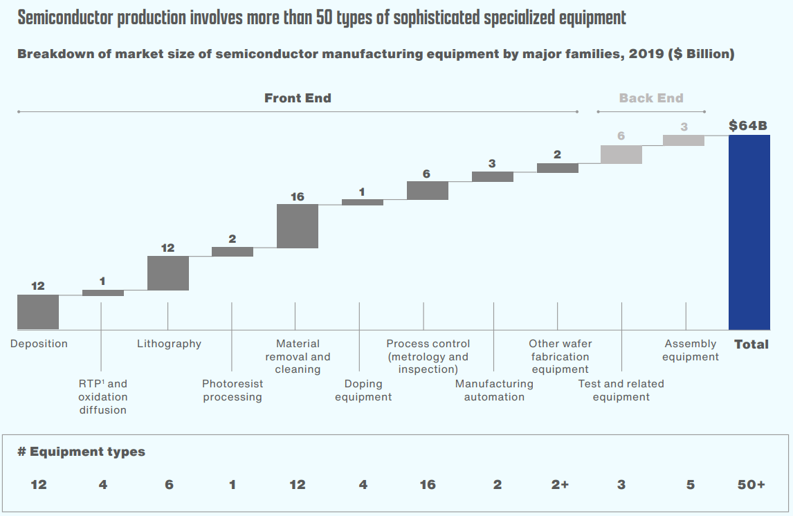
Semiconductor Process Control Equipment Market, valued at $6.4 billion in the year 2020 has been witnessing unprecedented growth in the last few years on the back of increasing defect of semiconductor equipment and hence demand of high accuracy in semiconductor equipment and increasing demand for miniaturisation of ICs.
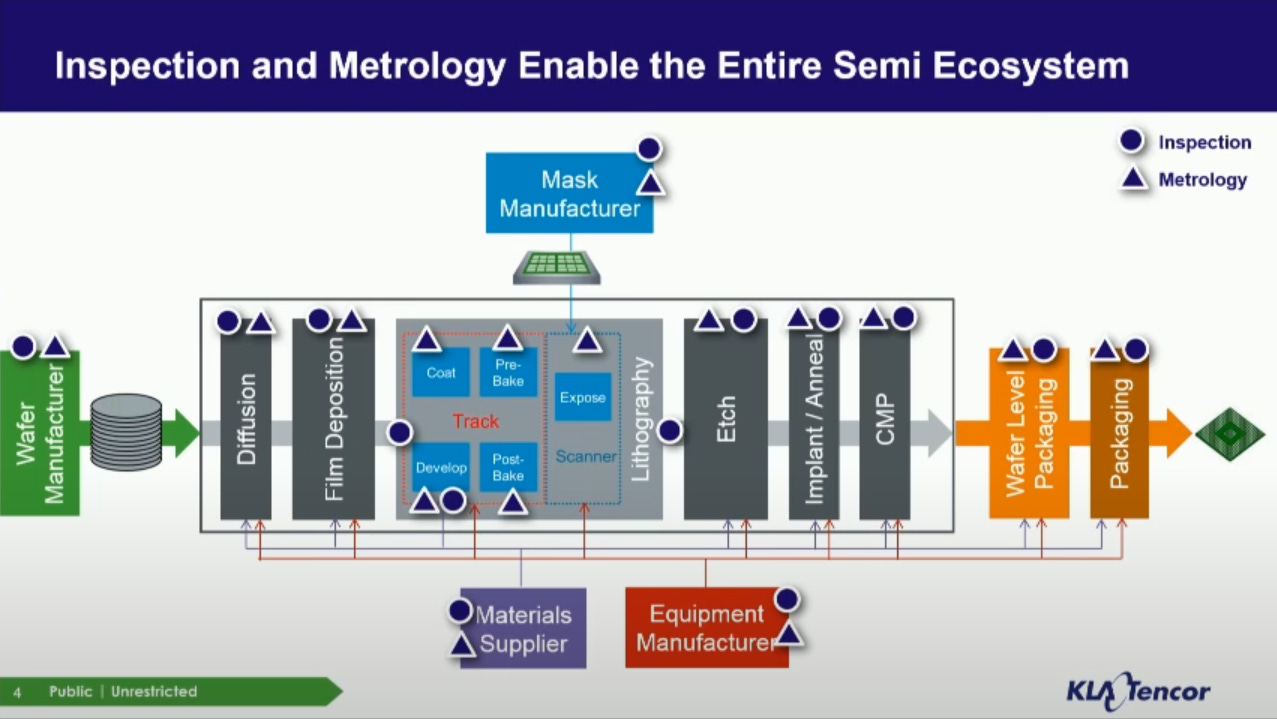
Inspection and Metrology
Inspection and Metrology are used in different parts of the semiconductor ecosystem. It’s used not only in the front end semiconductor fabs but also in photomask manufacturer, wafer manufacturer, materials supplier, equipment manufacturer and wafer packaging.
Process control equipment market, based on type, is fragmented into
inspection equipment,
metrology equipment, and
process control software.
Inspection is the process for detecting any particles or defects in a wafer. Metrology is a more comprehensive concept that refers not only to an act of measurement itself but to measurement performed by factoring in errors and accuracy, as well as the performance and mechanisms of metrology equipment.

Semiconductor device is completed through a large number of manufacturing processes. If a failure occurs during processing, the subsequent processing does not make sense. It is just to produce a defective product. Therefore, by inserting the inspection process to pivotal points of the manufacturing process, it will be advanced to the next step after confirming that there is no defect in the device. If the failure to the device is found, it interrupts the production, and then determines the cause and removes the defect. After the defect is sufficiently reduced, it is advanced to the next manufacturing step.
Inspection Equipment of Semiconductor Process Control Equipment occupies large segment globally due to the higher demand of inspection system in Process Control system and is expected to grow rapidly because of the increasing demand of more advanced Semiconductor Equipment. Foundries currently capture a sizeable portion of the overall industry share in Semiconductor Process Control Equipment.
Inspection Equipment
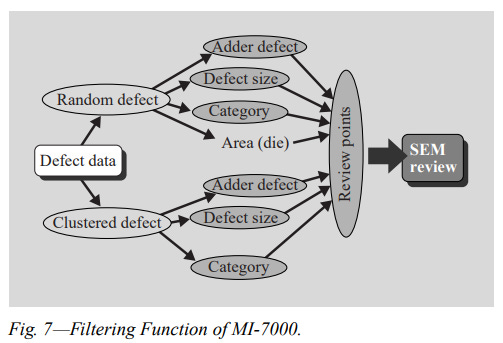
Equipment for detecting a defect of the device in the inspection process is the Semiconductor wafer defect inspection system. Defects in the semiconductor wafer manufacturing process are mainly small particles and pattern defects on the wafer. Semiconductor wafer defect inspection system detects physical defects (foreign substances called particles) and pattern defects on wafers and obtains the position coordinates (X, Y) of the defects. Specifying the position (coordinates) on the wafer of these particles or defects is the primary role of the inspection equipment. Defects can be divided into random defects and systematic defects.
Inspection can be performed on a patterned process wafer or on a bare wafer. Each of these has a different system configuration. There are many types of patterned wafer inspection systems, including the electron beam inspection systems, the bright-field inspection systems, and the dark-field inspection systems. Each of these has its own features, but the basic detection principles are the same. The non-patterned wafer inspection system is used in the wafer shipping inspection by wafer manufacturers, the wafer incoming inspection by device manufacturers and the equipment condition check using dummy bare wafers to monitor the cleanliness of equipment.
To capture the defects, chipmakers use e-beam and optical inspection tools. Both systems are used to find physical defects, such as voids, protrusions, and bridges in chips.
E-beam leverages the properties of electrons, while optical uses photons. Basically, an optical inspection system uses a broadband light source to illuminate a wafer. Then, the light is collected and an image is digitized, which helps find defects on the wafer.
In the fab, chipmakers use inspection systems for engineering analysis, critical line monitoring, and line monitoring.
E-beam inspection is used for engineering analysis in the R&D group. E-beam is used to find tiny and problematic defects during the early stages of chip development. Once those defects are rooted out and the chip meets spec, the device line moves to the fab.
Critical line monitoring is conducted in the fab. The goal is to find the most critical physical defects in patterned wafers. Line monitoring, which is also done in the fab, also detects defects in wafers. Both monitoring processes mainly use optical inspection. E-beam tools are also used sometimes.
Generally, e-beam inspection is used to detect physical defects that are too small for optical. E-beam inspection is also used for voltage-contrast defect applications. For this, an external bias is applied to a device. Then the e-beam analyzes the variations in the image contrast of the structure to locate shorts, opens and voids in chips.
Optical and E-Beam Wafer Inspection
E-beam and optical inspection are the two main technologies used to locate defects on a wafer. E-beam and optical tools are complementary technologies that perform different functions in the inspection flow.
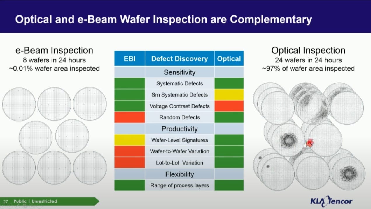
E-beam inspection (EBI) has very high resolution while low wafer throughput better for small systematic defect (defect that repeats a lot). E-beam inspection tools can detect two types of signals — backscattered electrons (BSE) and secondary electrons. BSE are electrons that originate from deeper parts of the structure. Secondary electrons come from the surface
Optical Inspection has low resolution but high throughput better for random defect, wafer level signatures, wafer to wafer variations in the same lot or different lots requires high speed optical inspection.
Optical inspection itself is split into two main segments, brightfield and darkfield. Darkfield inspection tools measure light reflected at a lower angle. Brightfield inspection, the workhorse technology in the fab, measures light at a higher angle. It uses broadband light to illuminate a wafer. Then, the light is collected and an image is digitized.
In the optical inspection market, Applied Materials, Hitachi High-Technologies, KLA and others compete in this arena.
The wafer inspection flow involves four parts—engineering analysis; critical line monitoring; line monitoring; and tool monitoring.
The inspection flow starts in R&D, where the goal is to capture as many defects as possible. For this, e-beam inspection is used to find the smallest defects, as the technology has sensitivities down to 3nm or lower.
The big market for wafer inspection is the physical defect arena. Both e-beam and optical inspection are used to find physical defects in R&D and the fab. Physical defects, the tiny and/or killer defects in a design, include voids, protrusions and bridges. At times, e-beam inspection can find tiny defects that can’t be caught by optical tools.
E-beam inspection won’t replace optical inspection in the fab. Chipmakers still want e-beam inspection tools in the flow, although they want systems with better resolutions and higher throughputs. While e-beam inspection is slow, next-generation tools promise to speed up the process, whether using a single- or multi-beam approach. Both types claim to find defects that other systems can’t detect.
Optical inspection is not exactly on its last legs, although the technology is being stretched to the limit somewhere between 20nm and 10nm.
ASML recently shipped a new multi-beam inspection system.
KLA re-entered the e-beam inspection market with a new and faster single-beam tool.
NuFlare and Tasmit are separately developing new e-beam inspection systems
Applied Materials, meanwhile, continues to offer its current single-beam e-beam inspection system
Applied and ASML compete in the e-beam inspection market.
Defect Review SEM
A Defect Review SEM is a Scanning Electron Microscope (SEM) that is configured to review defects found on a wafer. A defect detected by a semiconductor wafer defect inspection system is enlarged using an Review SEM to a high magnification image so that it can be reviewed and classified. A Defect Review SEM is mainly used together with the inspection systems in the production lines of electronic devices and other semiconductors.
AMAT, KLA & Hitachi Hitech compete in a related field called e-beam defect review
The overall wafer inspection market, including e-beam, optical and review tools, was a $3.04 billion business in 2019, according to VLSI Research. Of that figure, the optical inspection market is 11 times larger than the e-beam segment.
Metrology Equipment
Metrology equipment is the equipment for measuring the various dimensions of the semiconductor circuit patterns on a wafer.
CD-SEM to measure the width or diameter of the elements and patterns
Ellipsometer to measure film thickness of thin film
Overlay tool for measuring a displacement of the upper circuit pattern from the lower circuit pattern.
CD-SEM
A Critical Dimension SEM (CD-SEM: Critical Dimension Scanning Electron Microscope) is a dedicated system for measuring the dimensions of the fine patterns formed on a semiconductor wafer. Measurement of the line width and hole diameter of a circuit pattern at a specified location of a semiconductor wafer.
Critical dimension measurement is mainly performed in the following operations of the wafer fabrication process.
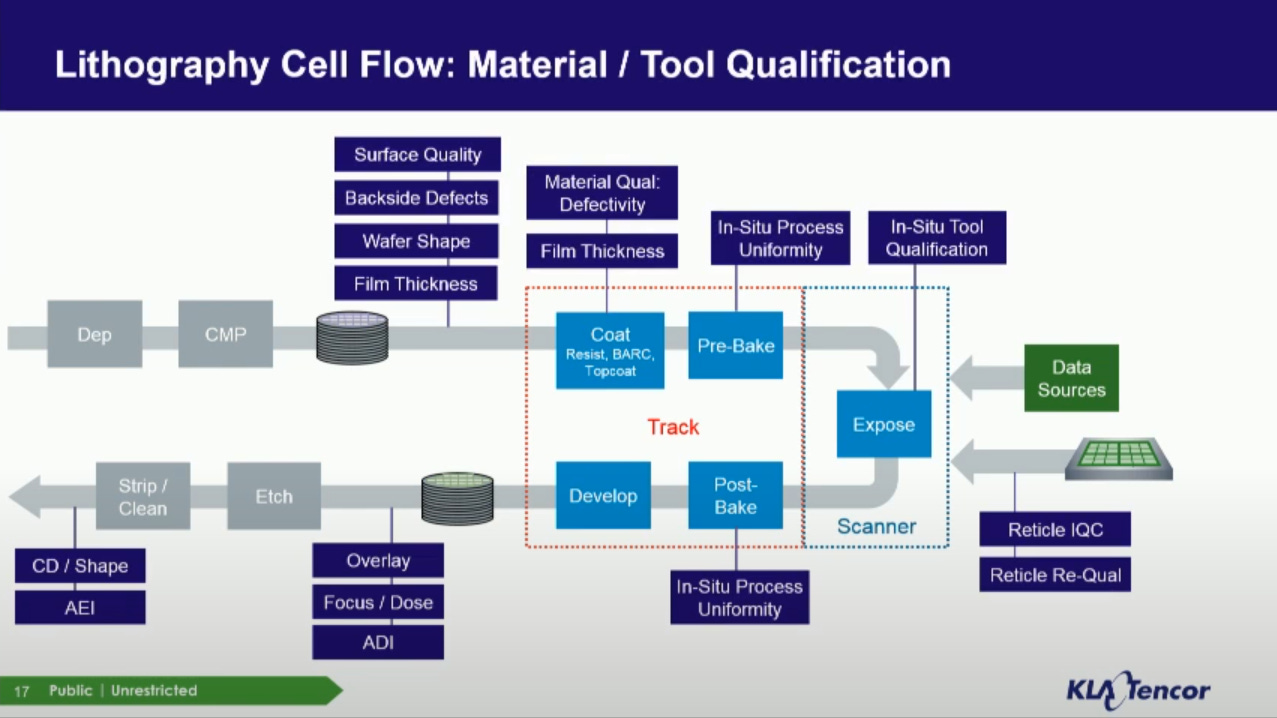
Measurement of photoresist pattern after exposure and development (ADI: After Development Inspection)
Measurement of the contact hole diameter / via-hole diameter and the wiring width after etching process (AEI: After Etch Inspection)
Thin Film Metrology
Measurement of the thickness of the thin films on the surface of a semiconductor wafer. Spectroscopic ellipsometry is a form of optical critical dimension (OCD) metrology. Spectroscopic ellipsometry looks at the properties of thin-film structures in logic and memory chips. Ellipsometry is a non-destructive, optical technique.
Overlay Metrology
Overlay Metrology system is used to check the accuracy of the overlay. Measurement is performed to check the accuracy of the shot overlay of the first and second layer patterns transferred onto a wafer.
Overlay Metrology uses optical imaging based overlay, Scatteromentry based overlay and Scanning Electron Microscope (SEM). .
Mask Inspection System
Mask Inspection System is a fab equipment that is used, before lithography, to inspect photomasks for defects during the production of semiconductor wafers.
Error-free reticles, or masks, are necessary to achieve high semiconductor device yields, since reticle defects can be replicated in every die on production wafers. These are high sensitivity reticle inspection, metrology and data analytics systems for mask blank manufacturers and reticle manufacturers (“mask shops”) to help them manufacture reticle blanks and patterned reticles that are free of defects and meet pattern placement and critical dimension uniformity specifications.
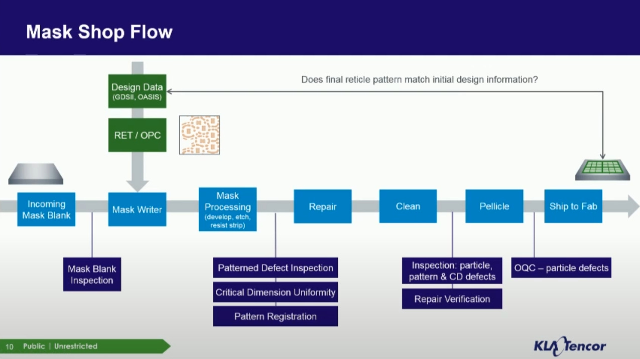
At the mask maker, a blank is processed into a photomask. To make a mask, the blank is patterned, etched, repaired and inspected. A pellicle is mounted on the mask, which is then shipped to the fab.
First, a system called an e-beam mask writer patterns the mask based on a given IC design. Then the mask is etched and cleaned.
At that point or before, an inspection system is used to look for defects. An inspection step is also performed at the end of the process. If a defect is detected, the defect can be repaired using a repair system. Not all defects can be repaired, however.
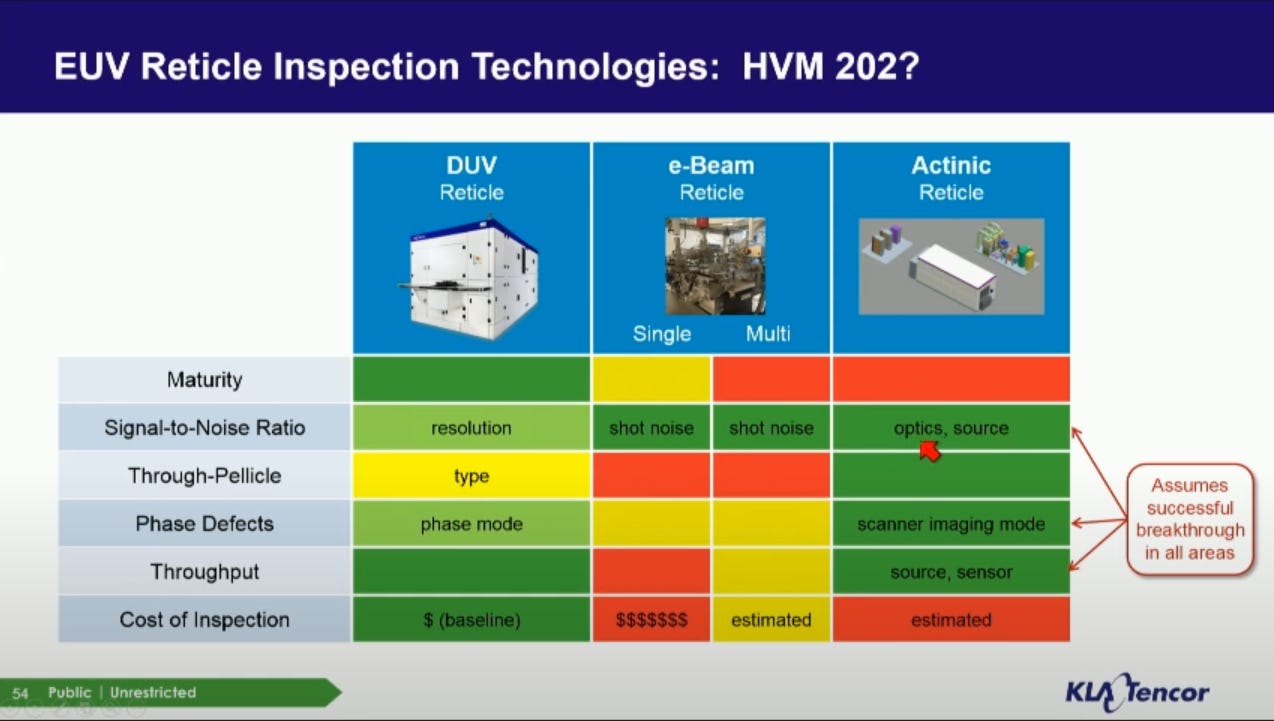
For optical masks, photomask makers use optical mask inspection systems for defect detection. Applied Materials, KLA, Lasertec and NuFlare sell optical-based mask inspection tools.
The problem with optical is resolution. Optical tools can handle current EUV masks, but they run out of steam around 20nm to 16nm half-pitch.
After the mask has been made, a pellicle is mounted on the reticle. Pellicles prevent particles from landing on the mask. A pellicle for optical masks is based on a thin polymer material. In comparison, ASML, the sole supplier of EUV pellicles, has developed a polysilicon-based pellicle that’s 50nm thick. The problem is that optical tools can’t inspect EUV masks with the pellicle on top. Unfortunately, the polysilicon-based material is opaque at 193nm wavelengths.
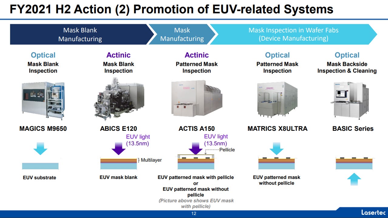
Meanwhile, at 7nm/5nm and beyond, Intel, Samsung and TSMC will require new inspection equipment beyond optical, namely actinic patterned mask inspection (APMI).
Unlike optical systems, APMI can inspect the EUV mask through an EUV pellicle. As a result, a mask maker doesn’t need to remove the pellicle to inspect the mask.
Process Control Equipment Landscape
The United States and Japan are the main producers of process control equipment. Defect inspection accounts for the 50% process control market followed by Metrology (CD SEM & Thin Film) and Mask Inspection.

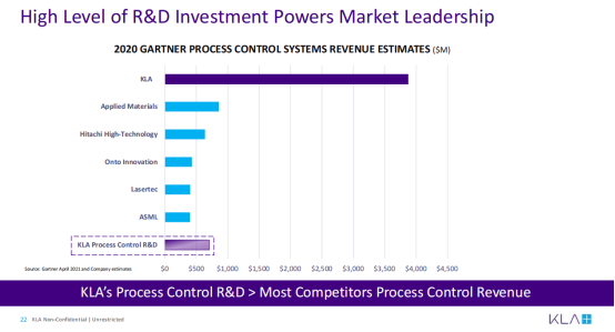
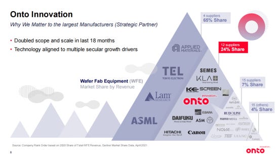
Process Control industry grew as a percent of overall wafer front-end equipment (WFE). KLA is the dominant player in the process control industry with a market share of 58% followed by Applied Materials(12%), Hitachi High Tech (8%) and ASML (6%) . Applied Materials primarily sells front end equipment in etch and deposition process while ASLM in photo lithography. Onto Innovation and Nova Measuring Instruments have a market share of 3.5% each.
Camtek and Bruker are the other smaller players in process control equipment market.
KLA
Nasdaq Symbol: KLAC, Market Cap: $44.95B, LTM Revenue: $6.45 billion, Gross Margins: 59.4%, Operating Margins:34.4%
KLA’s core franchise markets are Optical Wafer Inspection, Overlay Metrology and Mask Inspection. KLA is successful in re-entering into the e-beam inspection market with the first meaningful e-beam inspection revenue since 2015 with e-beam patterned wafer defect inspection system was launched during June, 2020.

Onto Innovation
Nasdaq Symbol: ONTO, Market Cap: $3.12B, LTM Revenue: $0.585 billion, Gross Margins: 52.5%, , Operating Margins:10.3%
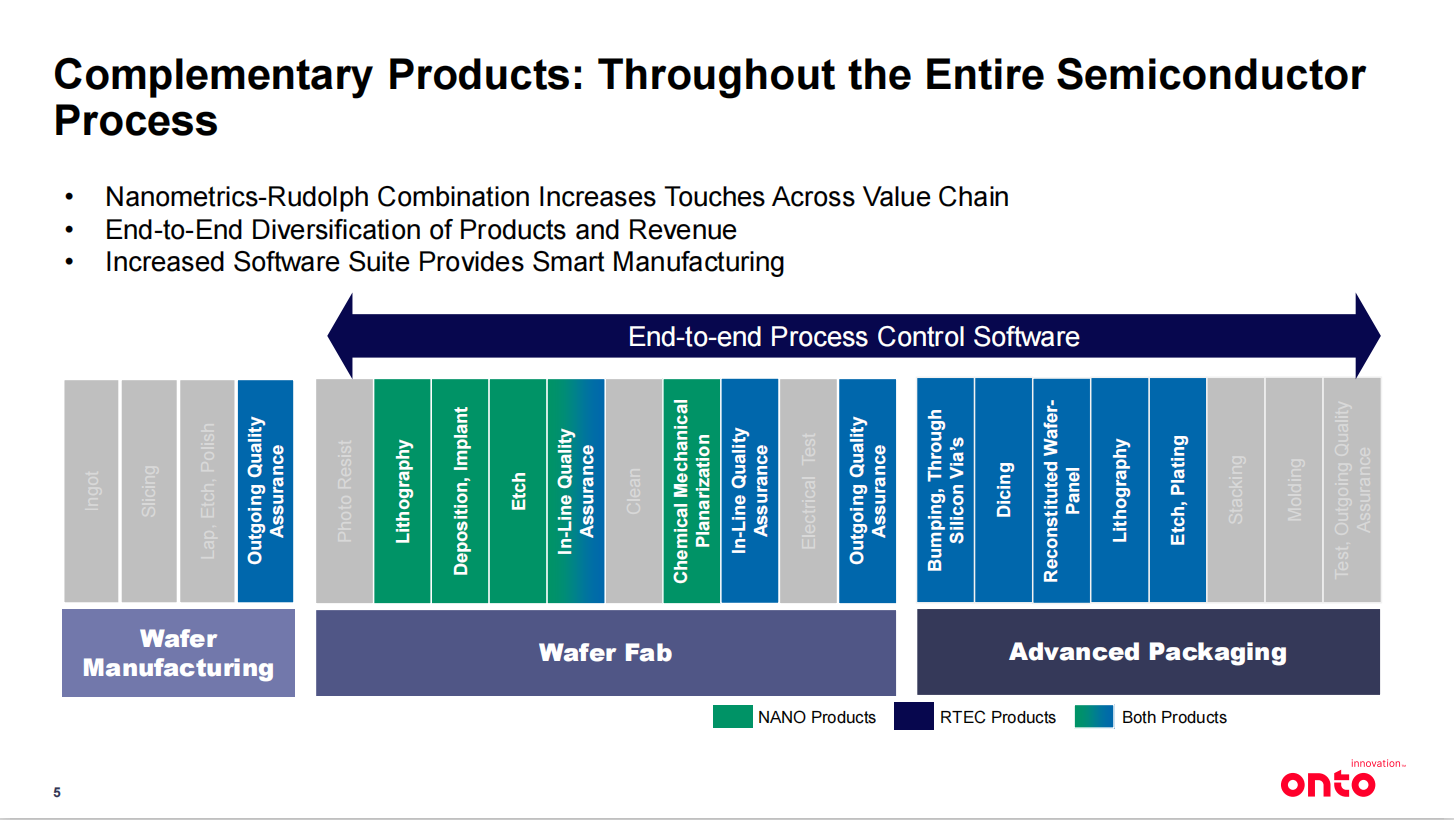
Nanometrics and Rudolph Technologies merged in Oct 2019 to form Onto Innovations. They had combined revenue of $556.94 million in 2020.
Onto Innovations manufacture process control systems for optical critical dimension metrology, thin film metrology, wafer inspection, 2D and 3D macro inspection and lithography tools for advanced packaging as well as advanced analytical software for semiconductor manufacturing.
Nova Measuring Instruments
Nasdaq Symbol: NVMI, Market Cap: $2.62B, LTM Revenue: $0.292 billion, Gross Margins: 56.9%, , Operating Margins:21.3%
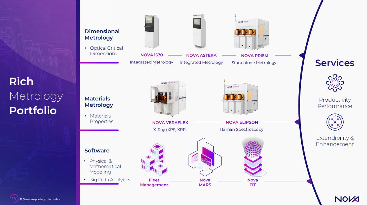
NOVA’s product portfolio includes a set of metrology platforms for dimensional, films, and material metrology measurements for process control for various semiconductor manufacturing process steps, including lithography, etch, chemical mechanical planarization, and deposition. Nova’s market offering is driven by product divisions: The Dimensional Metrology Division (DMD) which is responsible for optical technology-based metrology solutions (integrated and standalone), and the Materials Metrology Division (MMD) which is responsible for x-ray-based solutions.
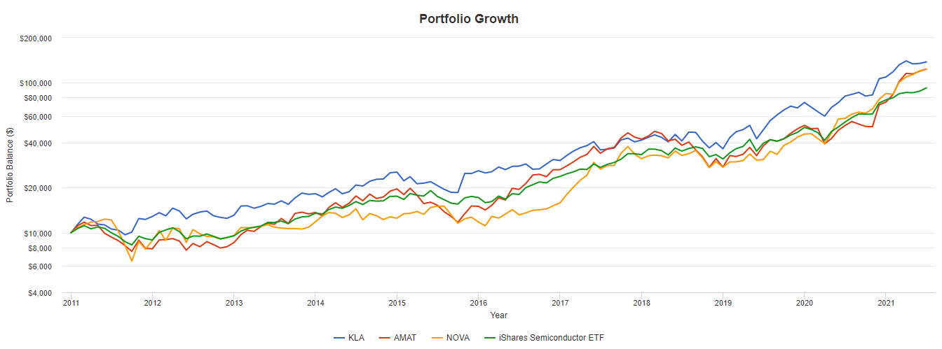
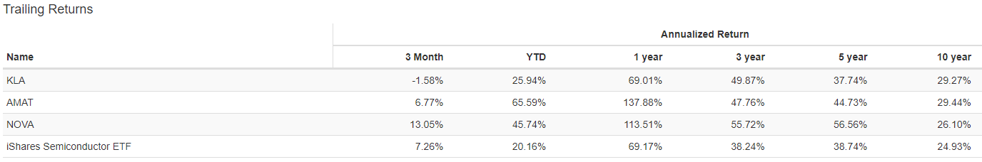
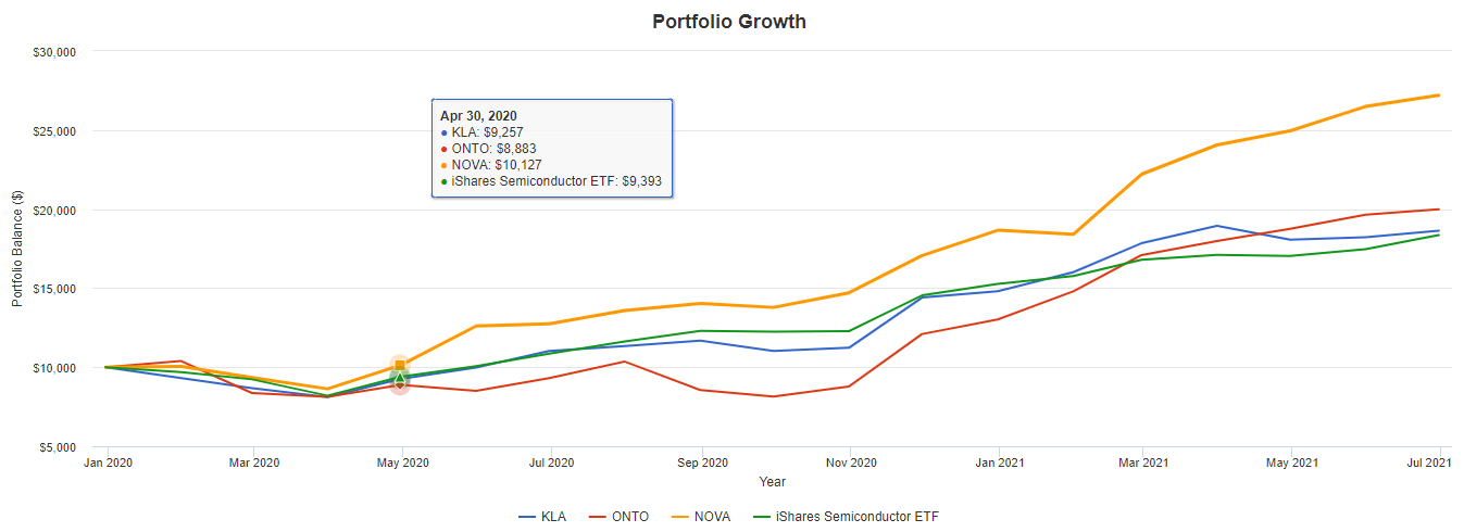
Stock Performance
All the US listed stocks in the process control market (KLAC, AMAT, ONTO & NVMI) are performing better than the bench iShares Semiconductor ETF. As Onto Innovations was listed only on Nov 2019 as merger of Nanometric and Rudolph Technologies, have taken this out from 10 year comparison.
Few of these process control companies will be analyzed at a later stage for investment purpose. We will discuss backend equipment companies in our next series.