Semiconductor Capital Equipment Overview : Part I
Semiconductor Front End Capital Equipment Overview
Welcome to Handsoff’s Newsletter by me, Handsoff Investor. Long term compounder buying great companies at bargain price.
I will be writing articles on companies that are in the semiconductor ecosystem. My first series will be a deep dive into the semiconductor equipment suppliers and will later on follow up with stock recommendations in the semiconductor equipment supplier space.
Sign up now so you don’t miss the first issue.
In the meantime, tell your friends!
Semiconductor Front End Capital Equipment Overview
Semiconductor Capital Equipment series is going to be divided into 8 parts:
Semiconductor Back End Capital Equipment Overview (Part III)
Front-end equipment suppliers: Etch, Deposition & Clean Process
Front-end equipment suppliers: Process Control
Front-end equipment suppliers: Lithography Process
Back-end equipment suppliers: Packaging
Back-end equipment suppliers: Assembling and Testing
Mule had already written good primer on Semiconductor Capital Equipment Series: Introduction, I will be complementing this by deep diving into each of the capital equipment suppliers and their process specialization. In this series I will give an overview of Semiconductor Ecosystem and front end equipment suppliers.
Semiconductor Ecosystem and Equipment Suppliers
The semiconductor fabrication process begins with a bare silicon wafer—a round disk that is typically 200 millimeters or 300 millimeters in diameter, about as thick as a credit card and gray in color. The process of manufacturing wafers is highly sophisticated and involves the creation of large ingots of silicon by pulling them out of a vat of molten silicon. The ingots are then sliced into wafers. Prime silicon wafers are then polished to a mirror finish.
The manufacturing cycle of an IC is grouped into three phases: design, fabrication and testing. Chip design process start with architectural layout of the circuit using Electronic Design Automation (EDA) software and the chips are manufactured by companies like TSMC, Samsung, Micron, etc. Equipment manufacturers that produce specialized equipment and machine tools for manufacturing, assembly, testing, and packaging. The equipment suppliers like ASML, Applied Materials, Lam Research, Tokyo Electron and KLA provides the equipment for front-end process. These specialized equipment are the most complex machines that humans have ever built which is very difficult to reverse engineer.
The fabrication of a chip is accomplished by depositing a series of film layers that act as conductors, semiconductors or insulators on bare wafers. The deposition of these film layers is interspersed with numerous other process steps that create circuit patterns, remove portions of the film layers, and perform other functions such as heat treatment, measurement and inspection. Most advanced chip designs require hundreds of individual steps, many of which are performed multiple times.
The majority of chips consist of two main structures: the lower structure, typically consisting of transistors or capacitors which perform the “smart” functions which is called Back End of Line (BEOL); and the upper “interconnect” structure, typically consisting of circuitry which connects the components in the lower structure which is called Front End of Line (FEOL). When the layers on the wafer have been fabricated, each chip on the wafer is tested for functionality using the process control equipment for inspection and metrology. The wafer is then cut into individual chips, and the chips that pass functional testing are packaged. Final testing is performed on all packaged chips. Packaged chips are then mounted onto PCBs for connection to the rest of the electronic system.
The demand for semiconductor capital equipment is triggered by the demand for chip supplier’s end product such as microprocessors or memory chips. Semiconductor revenue is expected to touch $1 trillion in 2030 compared to $450 billion in 2020 at a CAGR of 7-8%.
Demand from the Cloud, Internet of Things (IoT), and other markets is driving the need for increasingly powerful and cost-efficient semiconductors. This should boost the capital equipment spending which is at 13-14% of semiconductor revenue.
Chip Manufacturing Process
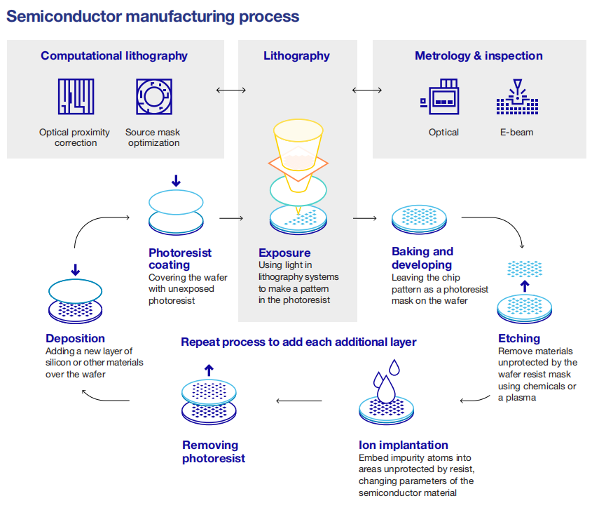
Chip manufacturing process is divided into wafer preparation, front-end processing and back-end processing. Front-end processing involves silicon wafer fabrication and other various functions such as photolithography, deposition, etching, cleaning, ion implantation, and chemical & mechanical polishing. Process control equipment is used for inspection, metrology and data analysis to remove defects to increase yield. Back-end processing encompasses the assembly, packaging and testing of integrated circuits.
Semiconductor equipment market segment includes Wafer Fab Equipment(WFE), Assembly & Packaging (A&P) and Test Equipment. Worldwide sales of semiconductor manufacturing equipment surged 19% from $59.8 billion in 2019 to a new all-time high of $71.4 billion in 2020.
The growth is expected to continue with the global semiconductor manufacturing equipment market reaching $71.9 billion in 2021 and $76.1 billion in 2022.
Wafer Fab Equipment
The Wafer Fab Equipment (WFE) segment in 2020 was $59.4 billion of which foundry and logic accounted for $30 billion, while NAND flash and DRAM manufacturing equipment was $14 billion and $15.4 billion respectively. Wafer Fab Equipment spending is expected to grow by 22-23% in 2021 based on the April 2021 forecast by Gartner and VLSI Research.
Top 5 wafer fab equipment companies are Applied Material, ASML, Lam Research, Tokyo Electron and KLA competing for $78 billion WFE market in 2021. Projected growth for 2022 is north of $85 billion.
Three companies accounted for over 50% of semiconductor capital spending in 2020. Samsung, the largest spender in 2020 at $27.9 billion, is expected to keep spending flat in 2021. TSMC will have the largest increase, adding $12.8 billion from 2020 to reach $30 billion in 2021, a 74% increase. TSMC will account for over 60% of the total industry spending increase of $20.4 billion. Intel has stated it will increase spending from $14.3 billion in 2020 to $19.5 billion in 2021, up 37%. The 2021 projections were mostly made in April after first quarter earnings release.
WFE market has been growing at 15% CAGR for the last 5 years with WFE mix favoring foundry and logic which will be beneficial for companies like ASML, Applied Materials and KLA. All the top 5 companies were less cyclical in the last 5 years which is expected to continue for the next decade. All these companies generate >25% revenue from the long term spares and service contract.
Top Nasdaq listed equipment companies
Now let’s look at the top 4 equipment companies listed in NASDAQ out of the below 15 and the market segments each one operate.
Applied Materials
Nasdaq Symbol: AMAT, Market Cap: $123.84B, R&D as % of Revenue: 13%
Applied provides manufacturing equipment, services and software to the semiconductor, display and related industries. The semiconductor systems segment includes semiconductor capital equipment used for many steps of the chip making process including the transfer of patterns into the device structure, transistors and interconnect fabrication, metrology, inspection and review and packaging technologies for connecting finished IC die.
Applied Materials has the leading market share of 50% in deposition process.
ASML
Nasdaq Symbol: ASML, Market Cap: $287.07B, R&D as % of Revenue: 15.7%
ASML provide chipmakers with hardware, software and services to mass produce patterns on silicon through lithography. A lithography system is essentially a projection system. Light is projected through a blueprint of the pattern that will be printed (known as a ‘mask’ or ‘reticle’) with the pattern encoded in the light, the system’s optics shrink and focus the pattern onto a photosensitive silicon wafer.
This process is repeated until the wafer is covered in patterns, completing one layer of the wafer’s chips. To make an entire microchip, this process is repeated layer after layer, stacking the patterns to create an integrated circuit (IC). The simplest chips have around 10 layers, while the most complex can have over 150 layers. The size of the features to be printed varies depending on the layer, which means that different types of lithography systems are used for different layers – latest-generation EUV systems for the most critical layers with the smallest features to DUV systems for less critical layers with larger features.
ASML have a dominant market share of 75% in the lithography equipment.
Lam Research
Nasdaq Symbol: LRCX, Market Cap: $89.03B, R&D as % of Revenue: 12.5%
Lam Research is a global supplier of innovative wafer fabrication equipment and services to the semiconductor industry. A strong global presence with core competencies in areas like nanoscale applications enablement, chemistry, plasma and fluidics, advanced systems engineering and a broad range of operational disciplines. Lam’s customer base includes leading semiconductor memory, foundry, and integrated device manufacturers (“IDMs”) that make products such as non-volatile memory (“NVM”), dynamic random-access memory (“DRAM”), and logic devices. Lam also address processes for back-end wafer-level packaging (“WLP”), which is an alternative to traditional wire bonding and can offer a smaller form factor, increased interconnect speed and bandwidth, and lower power consumption, among other benefits.
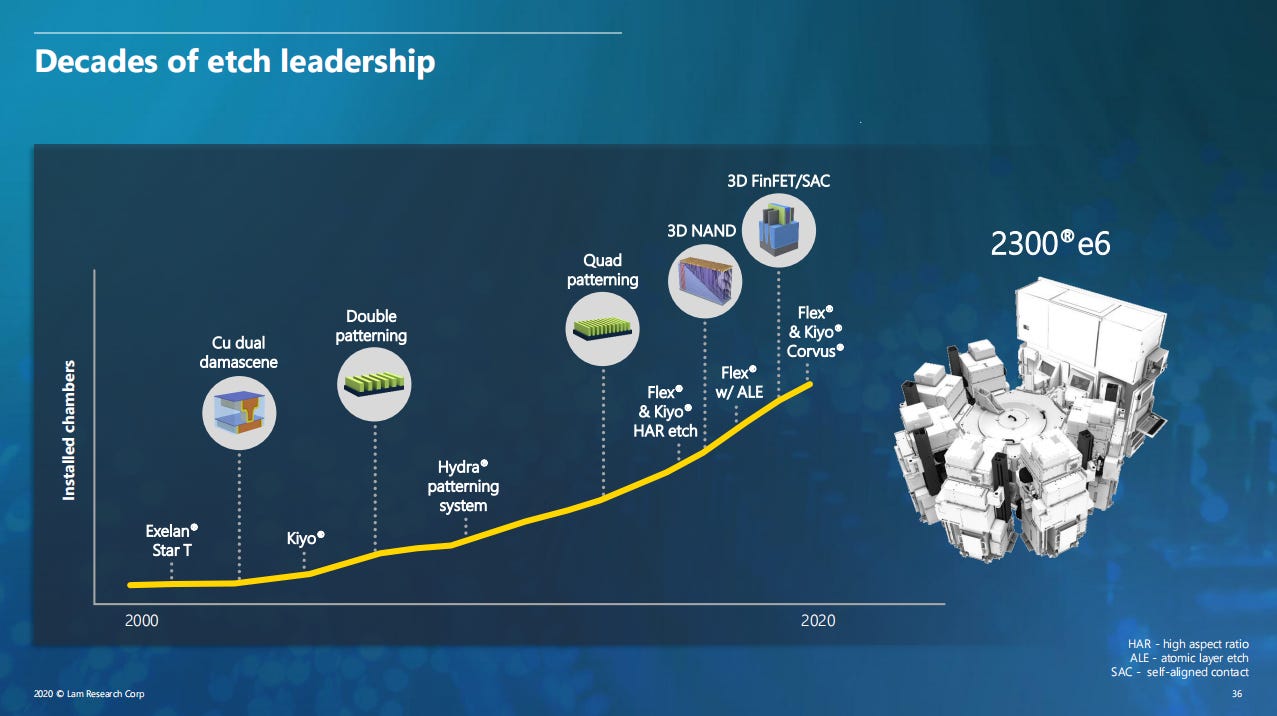
Lam is a market leader in Etch process.
KLA
Nasdaq Symbol: KLAC, Market Cap: $45.64B, R&D as % of Revenue: 15%
KLA develops industry-leading equipment for advanced process control and process-enabling solutions for manufacturing wafers, reticles, integrated circuits, packaging, printed circuit boards, and flat and flexible panel displays. KLA’s comprehensive portfolio of defect inspection, review, metrology, patterning simulation, in situ process monitoring and data analytics products, and related service, software and other offerings, helps substrate and chip manufacturers manage quality throughout wafer and chip fabrication processes.
KLA’s business is in the process control space of metrology and defect inspection with 62% of market share. KLA’s R&D spend in process control is more than the revenue of the nearest competition. They are expanding into packaging process control and PCB, Display and Component Inspection with the acquisition of Orbotech.
Stock Performance
The top equipment companies discussed (Applied Materials, ASML, Lam Research & KLA) are all 10 bagger over the last 10 years. ASML is toping the list as a 24 bagger due to it’s monopoly in lithography process.
We will discuss each of these companies in detail when we deep dive into the specific process like lithography, etch, deposition, clean and process control steps.


